
Originalmente concepito come tributo alla Core Rope memory cucita a mano dell'Apollo Guidance Computer, la mia idea è stata successivamente semplificata a "trova un modo per immagazzinare una breve stringa di caratteri in una serie di DIP switch, poi recuperala e mostrala su un display LCD tramite Arduino UNO".
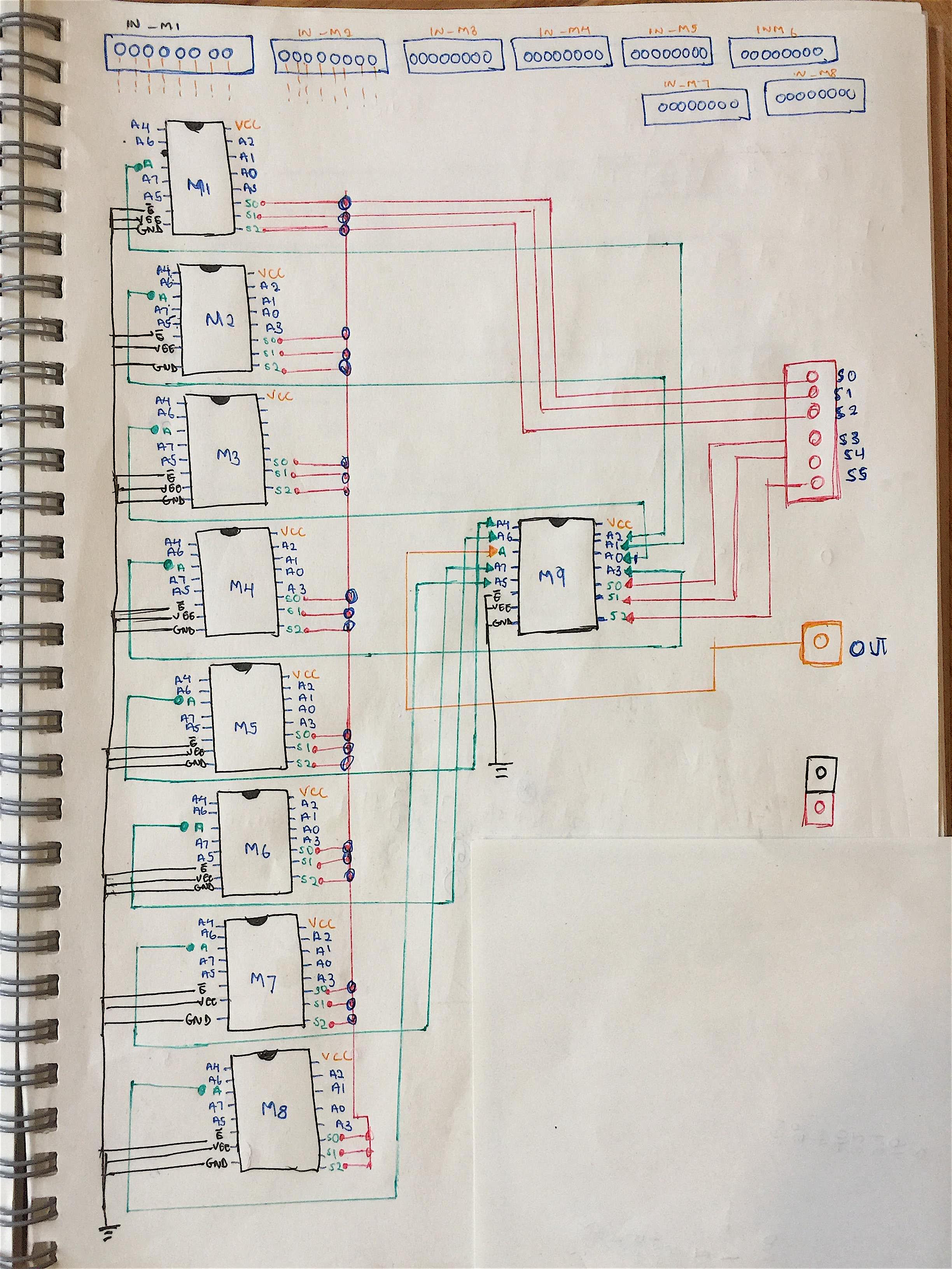
Sono stato ispirato dal (o meglio: ho plagiato il) progetto descritto qui: https://forum.arduino.cc/index.php?topic=446780.0: il prototipo si basa su un circuito molto semplice e su nove multiplexer a 8 canali connessi in modalità "daisy chain" (un multiplexer guida gli altri otto).
Considerato che ogni IC 4051 può gestire fino a 8 linee, il numero totale di bit nella ROM sarà 64 (8 Byte), con ogni bit settabile individualmente tramite il suo DIP switch. Un separato multiplexer 4051 legge uno a uno i bit di ogni Byte, quello rimanente seleziona quale Byte leggere.
La ROM sarà testata memorizzando 8 Byte di testo come caratteri ASCII, che saranno mostrati da Arduino su un display LCD a 2 linee.
Originally conceived as a tribute to the hand-sewn Core Rope memories of the Apollo Guidance Computer, my idea was successively simplified to "find a way to store a short character string in a series of DIP switches, then retrieve and display that text via an Arduino UNO".
I was inspired by (or better: I plagiarized) the project described here: https://forum.arduino.cc/index.php?topic=446780.0: the prototype is based on a very simple circuit and nine 8-channel multiplexers in a "MUX daisy chain" arrangement (one multiplexer drives the other eight).
Considering that each 4051 IC can manage up to 8 lines, the total number of bits in the ROM will be 64 (8 Byte), with each bit set independently via its own dip switch. A separate 4051 multiplexer reads one by one the bits in each Byte, the remaining one selects which byte to read.
The ROM will be tested by storing 8 Byte of text as ASCII characters, that will be displayed by Arduino on a 2 line LCD display.
|
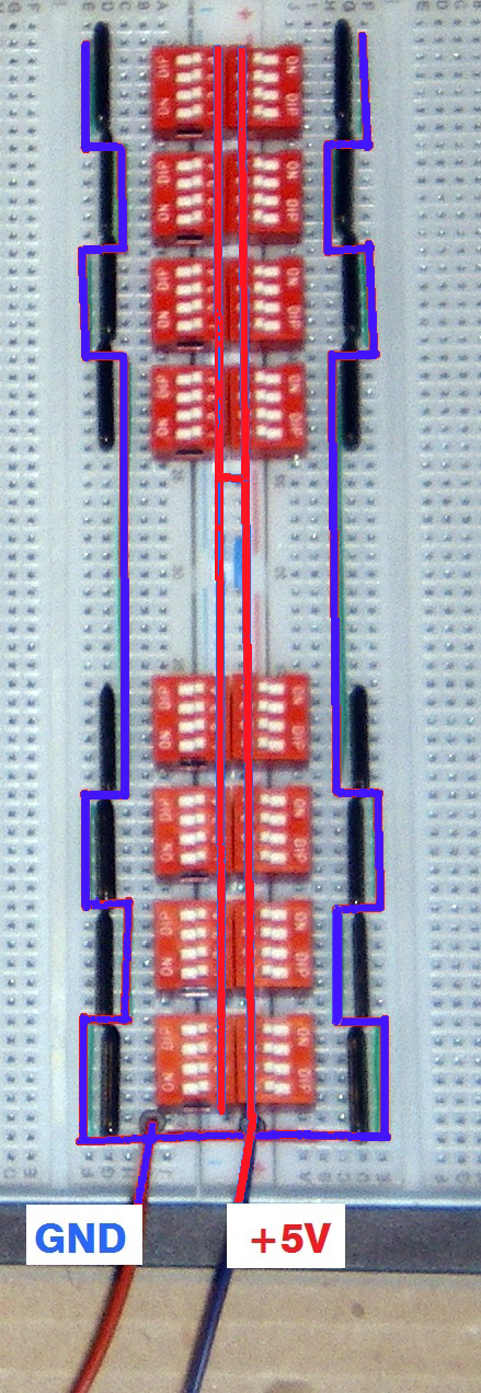
Per ogni Byte, sono a disposizione due banchi da 4 DIP switch. La scelta di blocchi da 4 interruttori è stata dettata solo dalla convenienza economica (...una svendita). |
|
For each Byte, two banks of 4-bit DIP switches are provided. The choice of 4-switch packages has been dictated only by economic convenience (...a sale). |
|
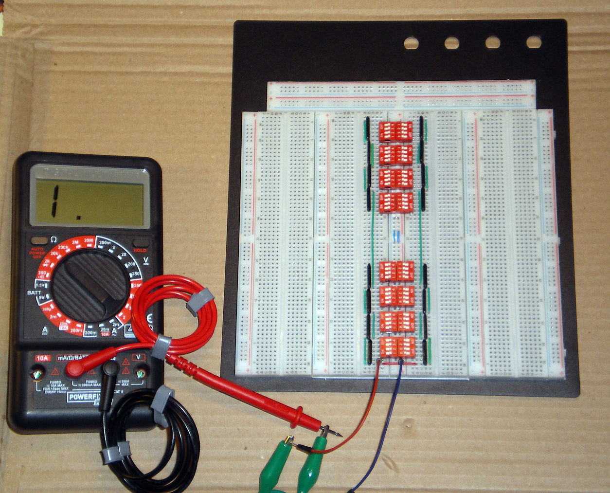
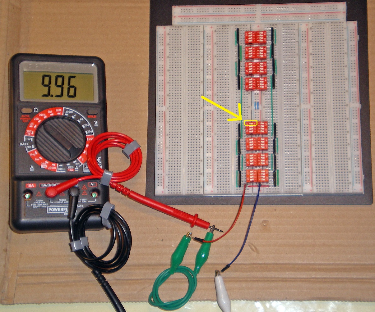
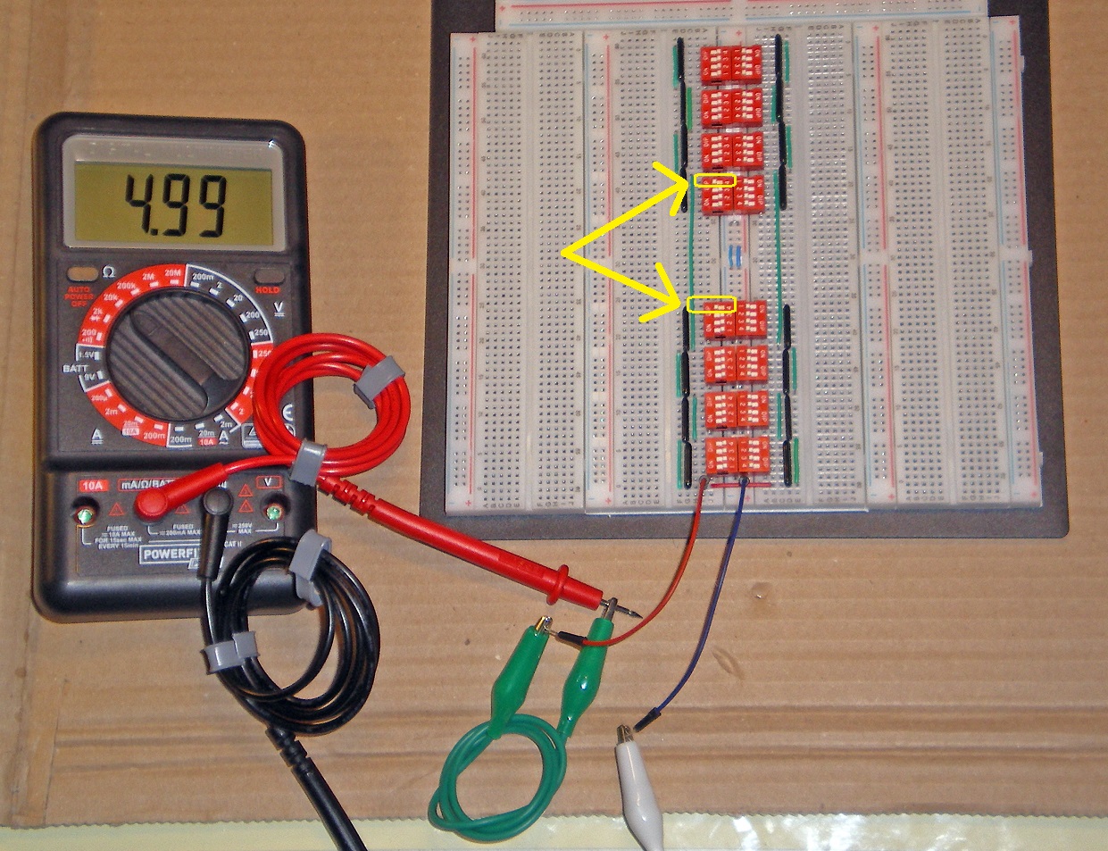
La continuità del circuito interno è stata testata molto facilmente: con tutti gli switch aperti, il circuito nel suo assieme è aperto. Chiudere ogni singolo switch comporta una lettura di 10 KΩ, chiudere una qualsiasi coppia dà una letture di 5 KΩ, e così via. |
|
Inner circuit continuity was tested very easily: with all switch open, the circuit as a whole is open. Closing any single switch gives a reading of 10 KΩ, closing any two gives a reading of 5 KΩ, and so on. |
|
||
|
|
||
|
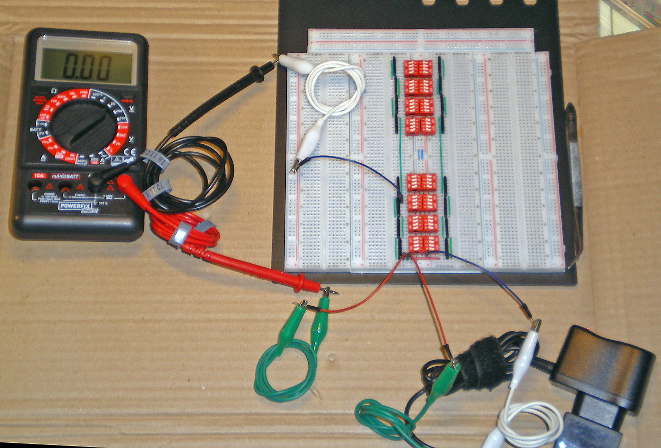
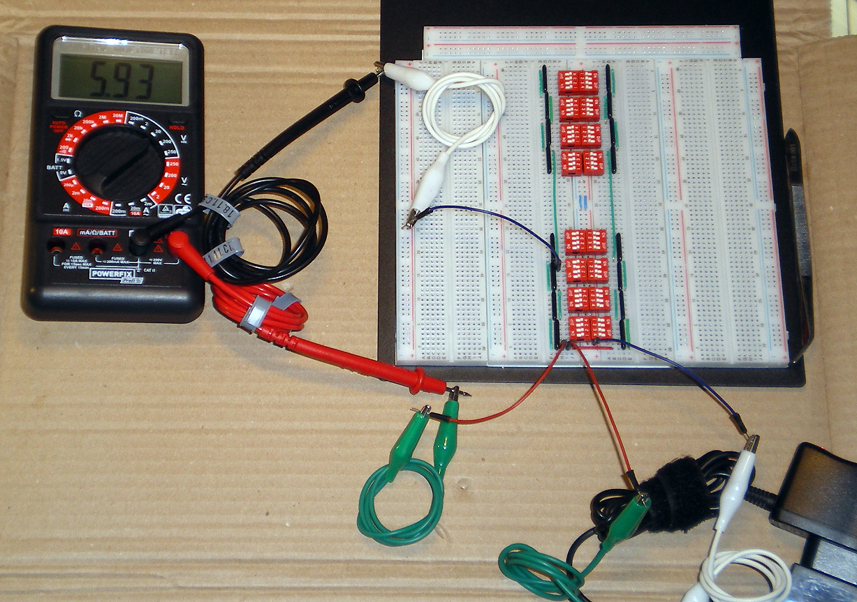
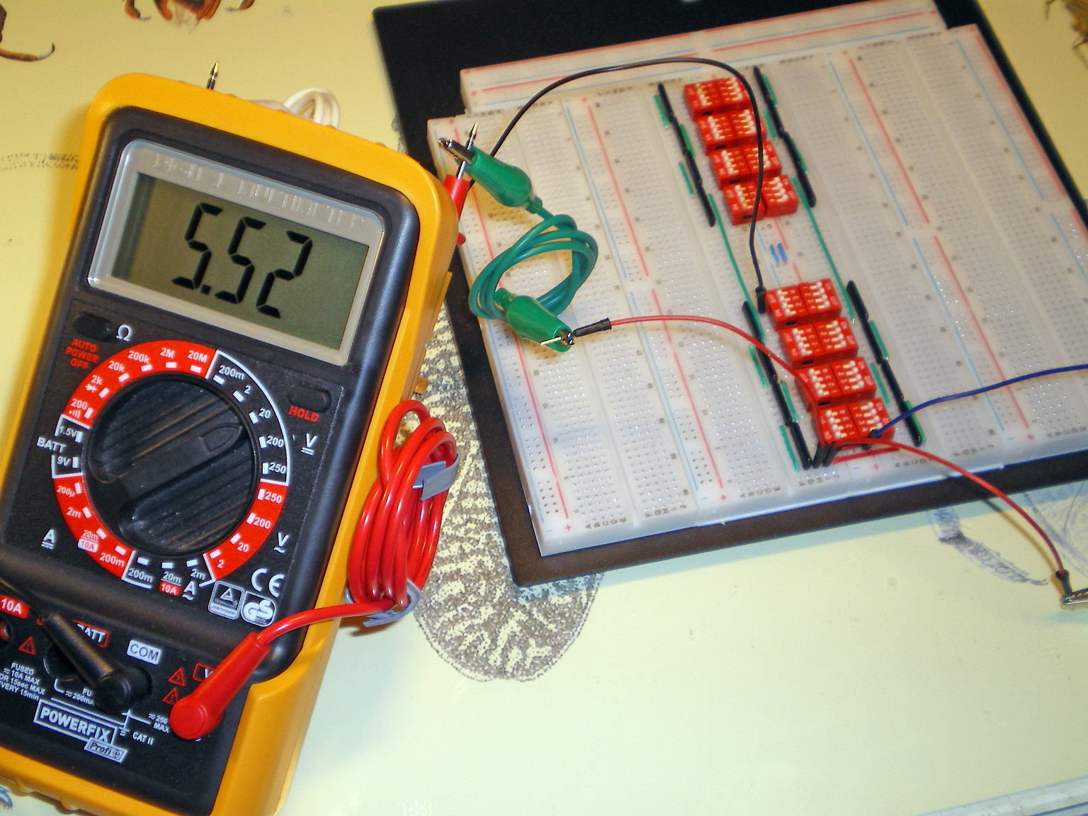
Considerato che l'intero progetto riguarda scansire bit per bit la ROM, per ottenere una lettura "high" per ogni interruttore chiuso ("bit alto"), mi serve un circuito in cui il voltaggio risente il meno possibile del numero di interruttori chiusi. Essendo privo delle nozioni di base, ho dovuto verificare il voltaggio in varie configurazioni della ROM. Destra: tutti gli switch chiusi, nessun flusso di corrente in alcuna linea |
|
Considering that the whole project is about scanning bit by bit the ROM, to get an "high" reading for each closed switch (high bit), I need a circuit where the voltage is affected as little as possible by the number of closed switches. Lacking basic notions, I needed to check the voltage in different ROM configurations. Left: all switches closed, no current flow in any line |
Destra: un interruttore chiuso, lettura 5.93 V |
|
Left: one switch closed, 5.93 V reading |
Destra: tutti gli interruttori chiusi,lettura 5.52 V in qualsiasi linea |
|
Left: all switches closed, 5.52 V reading in any line |
|
Lo "stadio di controllo" (qui citato anche come "circuito esterno") coi multiplexer connessi a margherita si è ispirato allo schema a destra, di PaulRB dal seguente post nel forum di Arduino: https://forum.arduino.cc/index.php?topic=446780.0 in cui Arduino è utilizzato per controllare 64 linee in un processo a due passi:
|
|
The "control stage" (here also cited as "outer circuit") by daisy-chained multiplexers was inspired by the schematics on the left, by PaulRB from the following Arduino forum post: https://forum.arduino.cc/index.php?topic=446780.0 where Arduino is used to control 64 lines in a two-step process:
|
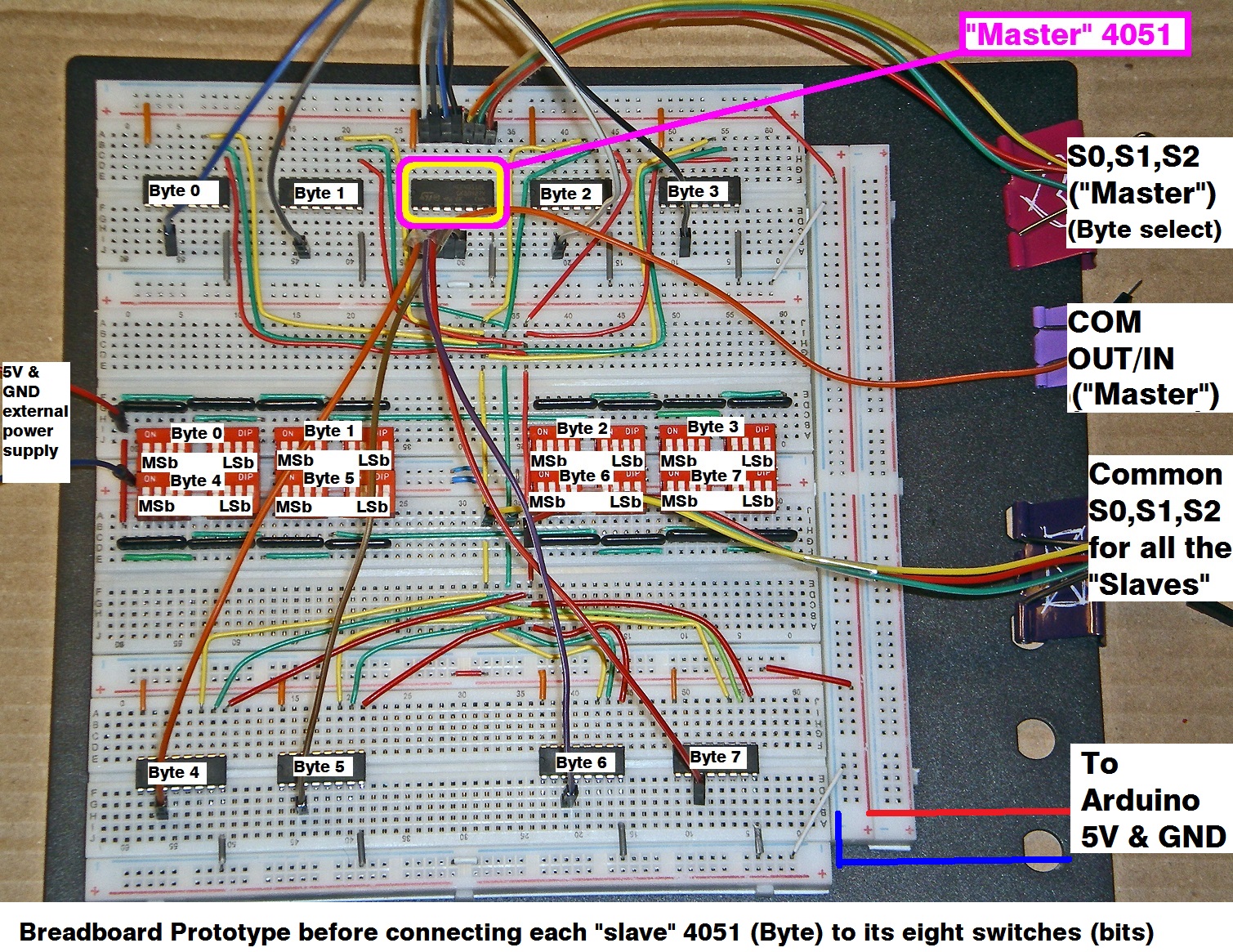
Ho messo lo schema su breadboard come illustrato a destra: la foto e il prototipo Fritzing non includono le connessioni tra ogni 4951 "slave" (Byte) e i suoi 8 DIP Switch ("bit"), che sono ovviamente necessarie per far funzionare il prototipo ma che renderebbero l'immagine illeggibile. Anche la connessione a ground dei pin 6 e 7 in ogni 4051 manca dalla fotografia, come pure i ponticelli per ripristinare la continuità delle linee di alimentazione in alto, interrotte alla mezzeria. |
|
I breadboarded the schematics as illustrated at left: the photo and the Fritzing prototype do not include the lines between each "slave" 4051 (Byte) and its 8 DIP switches ("bits"), that are obviously needed to make the prototype work but that would make the picture unreadable. Also the connection to ground of pin 6&7 in each 4051 are missing from the photo, as well as the "bridges" to restore continuity of the topmost horizontal power rails, interrupted at midway. |
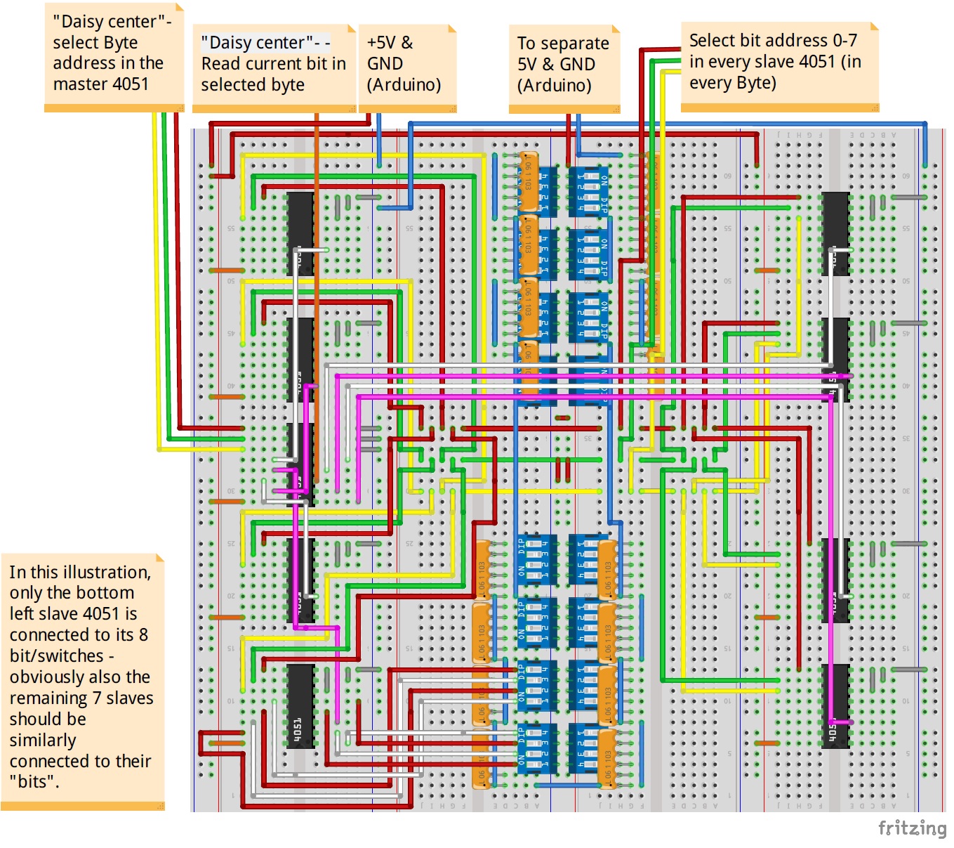
Destra: Schema Fritzing con il solo "Byte" 0 connesso ai suoi "bit" |
|
Left: Fritzing schema with only "Byte" 0 connected to its "bits" |
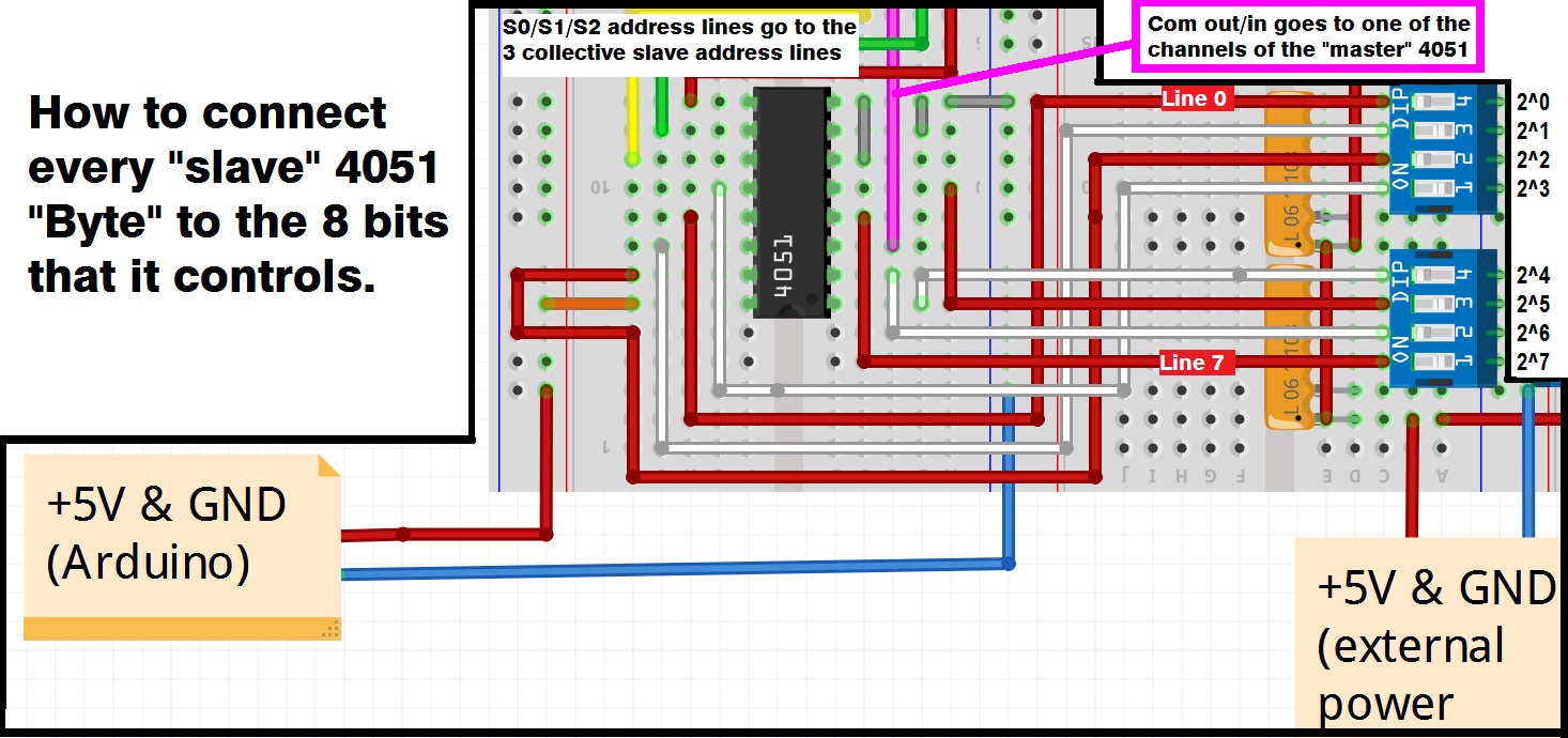
Destra: Dettaglio della connessione tra ciascun "Byte" 0 e i suoi "bit" |
|
Left: Detail of the connection between each "Byte" and its "bits" |
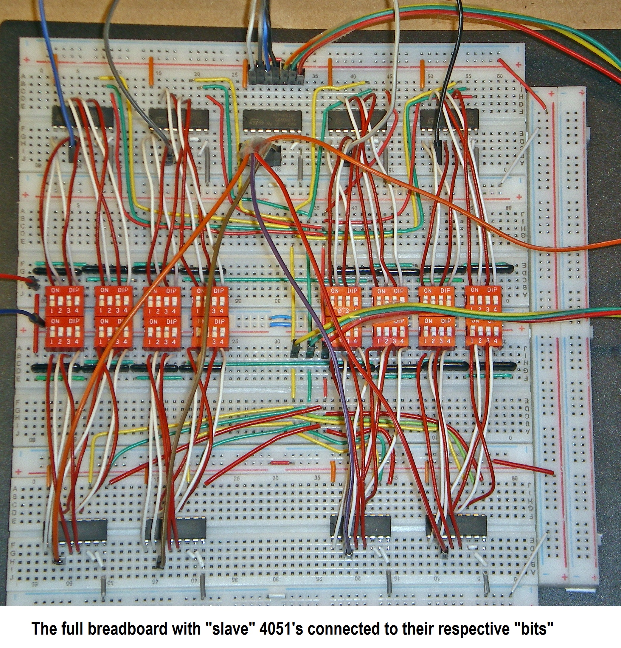
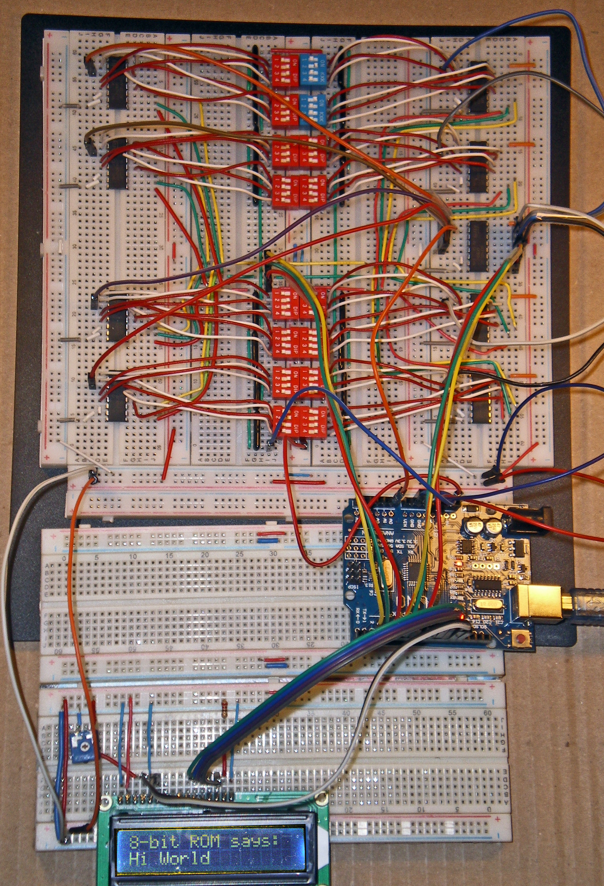
Destra: L'intera breadboard con ogni "Byte" connesso ai suoi "bit"L'immagine a destra è stata scattata con il circuito interno ancora collegato a un alimentatore esterno con polarità invertita. Voglio ribadire che:
|
|
Left: The full breadboard with each "Byte" connected to its "bits"The picture at left was taken with the inner circuit still attached to an external power supply with reversed polarity. I want to state again that:
|
Destra: Il prototipo completamente assemblato, comprensivo di un display LCD che mostra i contenuti della ROM da 8 Byte |
|
Left: the fully assembled prototype, including an LCD display that shows the content of the 8-Byte ROM |
|
Sommario per la costruzione |
|
Manufacturing summary |
/*

DIP/DIL Switch-based 8-Byte ROM via daisy-chained 4051 multiplexers and Arduino

Circuit and comments:
See http://www.cesarebrizio.it/Arduino/DIP_Switch_ROM.html
Circuit is as illustrated here: http://www.cesarebrizio.it/Arduino/Final%20Fritzing%20Schema.jpg

 created 03 Feb 2019
 by Cesare Brizio
 modified ----

This example code is in the public domain.

Originally conceived as a tribute to the hand-sewn Core Rope memories of the Apollo Guidance Computer,
my idea was successively simplified to "find a way to store a short character string in a series of
DIP switches, then retrieve and display that text via an Arduino UNO".

I was inspired by (or better: I plagiarized) the project and the schematics by PaulRB described here:

https://forum.arduino.cc/index.php?topic=446780.0

I have 64 DIP switches, each one capable of storing a bit of information, in eaght groups of eight switches
(closed = non-null voltage reading = binary 1 - opened = null voltage reading = binary 0)

Each group of eight switches, that I will call a "Byte", is connected to the eight I/O channels of a
separate "slave" 4051.

The three address lines S0/S1/S2 of all the slave multiplexers are common: one S0, one S1, and one S2 address all
the slave multiplexers simultaneously

I am using a master multiplexer 4051 whose I/O channels are connected to the com out/in of each slave multiplexer
Thus, by a two-step process:
a) select the "byte" (=slave multiplexer) to read via the S0/S1/S2 of the master 4051
b) select which "bit" to read from each slave via the common S0/S1/S2 of the slave 4051's
I can access one switch at a time and make individual reading.

As each byte is meant to store an 8-bit ASCII character, I compose the bytes by the successive readings from
their bits, and translate them into ASCII values, that are added to the string.

The string obtained is displayed on an LCD display driven by Arduino.

By changing the open/closed DIP switch configuration, I can vary the displayed string in real time.


  ==========================
  The circuit for LCD board:
  ==========================
 * LCD RS pin to digital pin 15
 * LCD Enable pin to digital pin 14
 * LCD D4 pin to digital pin 5
 * LCD D5 pin to digital pin 4
 * LCD D6 pin to digital pin 3
 * LCD D7 pin to digital pin 2
 * LCD R/W pin to ground
 * LCD VSS pin to ground
 * LCD VCC pin to 5V
 * 10K resistor:
 * ends to +5V and ground
 * wiper to LCD VO pin (pin 3)

*/
// include the library code:
#include <LiquidCrystal.h>

// initialize the library with the numbers of the interface pins
const int rs = 13, en = 12, d4 = 11, d5 = 10, d6 = 9, d7 = 8;
LiquidCrystal lcd(rs, en, d4, d5, d6, d7);

// "Slave" 4051 ADDRESS PINS :
int slave_S0 = 2;
int slave_S1 = 3;
int slave_S2 = 4;

// "Master" 4051 ADDRESS PINS :
int master_S0 = 5;
int master_S1 = 6;
int master_S2 = 7;

//
int analogPin = A0;

int ReadVolt = 0;

int bitValue;

int asciiCode;

char asciiChar ="";

int powerOfTwo = 0;

char asciiString[8];


void setup() {
    // set up the LCD's number of columns and rows:
    lcd.begin(16, 2);
    // Print a message to the LCD.
    lcd.print("8-bit ROM says: ");
    // CONFIGURE ADDRESS PINS
    pinMode(master_S0, OUTPUT);
    pinMode(master_S1, OUTPUT);
    pinMode(master_S2, OUTPUT);
    pinMode(slave_S0, OUTPUT);
    pinMode(slave_S1, OUTPUT);
    pinMode(slave_S2, OUTPUT);

  Serial.begin(9600);

}


void loop() {

    for( int x = 0; x < 8;  ++x )
          asciiString[x] = (char)0;


    // For each "Byte"
    for (int i = 0; i < 8; i++) {

        // Select current Byte
        cycle4051('M',i);

        delay(5);

        //Serial.print("Byte ");
        //Serial.print(i);
        //Serial.println(" readings:");
        //Serial.print(">");

        asciiCode=0;

        for (int j = 7; j >=0; j--) {

            // Select current bit
            cycle4051('S',j);

            delay(5);

            ReadVolt = analogRead(analogPin);

            if(ReadVolt>500) // check if current is running
            {
                bitValue=1; // Switch closed, bit high
                asciiCode = asciiCode + powerOfTwo;
            }
            else
            {
                bitValue=0; // Switch open, bit low
            }

            //Serial.print(bitValue);
            //Serial.print(ReadVolt);
            //Serial.print("|");

        }

        //Serial.print(asciiCode);
        //Serial.println("|");
        asciiString[i]=asciiCode;


    }
    //Serial.println("--- End series");
    //Serial.println(asciiString);

    for( int z = 0; z < 8;  ++z )
        {
        // (note: line 1 is the second row, since counting begins with 0):
        lcd.setCursor(z, 1);
        // print on the LCD the current character from the string:
        lcd.print(asciiString[z]);
        // print it also on the Serial Monitor
        Serial.print(asciiString[z]);
        }
    Serial.println("");
    delay(10);
}


void cycle4051(char master_slave, int stepNumber) {
     // It's very obvious that this subprogram could have been written in
     // a much more compact form. I prefer to use a more verbose style
     // for clarity, readability and ease of maintenance.
     // I do know that there are may valid alternatives to the stratagem of
     // using the powerOfTwo variable - the native POW() exponentiation function
     // that I could well have used has its drawbacks.
     switch (master_slave) {
        case 'M':
            //Next "Byte" (= next slave 4051)
            //Select the next slave 4051, connected to one of the channels of the master 4051
            switch (stepNumber) {
               case 0:
                   //Select Channel 0 of the master 4051
                   digitalWrite(master_S2, LOW);
                   digitalWrite(master_S1, LOW);
                   digitalWrite(master_S0, LOW);
                   break;
               case 1:
                   //Select Channel 1 of the master 4051
                   digitalWrite(master_S2, LOW);
                   digitalWrite(master_S1, LOW);
                   digitalWrite(master_S0, HIGH);
                   break;
               case 2:
                   //Select Channel 2 of the master 4051
                   digitalWrite(master_S2, LOW);
                   digitalWrite(master_S1, HIGH);
                   digitalWrite(master_S0, LOW);
                   break;
               case 3:
                   //Select Channel 3 of the master 4051
                   digitalWrite(master_S2, LOW);
                   digitalWrite(master_S1, HIGH);
                   digitalWrite(master_S0, HIGH);
                   break;
               case 4:
                   //Select Channel 4 of the master 4051
                   digitalWrite(master_S2, HIGH);
                   digitalWrite(master_S1, LOW);
                   digitalWrite(master_S0, LOW);
                   break;
               case 5:
                   //Select Channel 5 of the master 4051
                   digitalWrite(master_S2, HIGH);
                   digitalWrite(master_S1, LOW);
                   digitalWrite(master_S0, HIGH);
                   break;
               case 6:
                   //Select Channel 6 of the master 4051
                   digitalWrite(master_S2, HIGH);
                   digitalWrite(master_S1, HIGH);
                   digitalWrite(master_S0, LOW);
                   break;
               case 7:
                   //Select Channel 7 of the master 4051
                   digitalWrite(master_S2, HIGH);
                   digitalWrite(master_S1, HIGH);
                   digitalWrite(master_S0, HIGH);
                   break;
            }
            break;
        case 'S':
            //Next "bit" (= next channel in the currently selected slave 4051)
            //Select the next channel of the slave 4051, connected to one of the dip switches
            switch (stepNumber) {
               case 0:
                   //Select Channel 0 of the slave 4051
                   digitalWrite(slave_S2, LOW);
                   digitalWrite(slave_S1, LOW);
                   digitalWrite(slave_S0, LOW);
                   powerOfTwo=1;
                   break;
               case 1:
                   //Select Channel 1 of the slave 4051
                   digitalWrite(slave_S2, LOW);
                   digitalWrite(slave_S1, LOW);
                   digitalWrite(slave_S0, HIGH);
                   powerOfTwo=2;
                   break;
               case 2:
                   //Select Channel 2 of the slave 4051
                   digitalWrite(slave_S2, LOW);
                   digitalWrite(slave_S1, HIGH);
                   digitalWrite(slave_S0, LOW);
                   powerOfTwo=4;
                   break;
               case 3:
                   //Select Channel 3 of the slave 4051
                   digitalWrite(slave_S2, LOW);
                   digitalWrite(slave_S1, HIGH);
                   digitalWrite(slave_S0, HIGH);
                   powerOfTwo=8;
                   break;
               case 4:
                   //Select Channel 4 of the slave 4051
                   digitalWrite(slave_S2, HIGH);
                   digitalWrite(slave_S1, LOW);
                   digitalWrite(slave_S0, LOW);
                   powerOfTwo=16;
                   break;
               case 5:
                   //Select Channel 5 of the slave 4051
                   digitalWrite(slave_S2, HIGH);
                   digitalWrite(slave_S1, LOW);
                   digitalWrite(slave_S0, HIGH);
                   powerOfTwo=32;
                   break;
               case 6:
                   //Select Channel 6 of the slave 4051
                   digitalWrite(slave_S2, HIGH);
                   digitalWrite(slave_S1, HIGH);
                   digitalWrite(slave_S0, LOW);
                   powerOfTwo=64;
                   break;
               case 7:
                   //Select Channel 7 of the slave 4051
                   digitalWrite(slave_S2, HIGH);
                   digitalWrite(slave_S1, HIGH);
                   digitalWrite(slave_S0, HIGH);
                   powerOfTwo=128;
                   break;
            }
            break;
    }


}
❦